
Group participants:
Glebova N. V., Illarionov Yu. Yu., Tyaginov S. E., Vexler M. I.
Formation:
The group is active since mid-1980s. During many years it was headed by the senior researcher Dr. A.F. Shulekin; after his retirement (since 2005), Dr. M.I. Vexler became a group leader. Mr. Tyaginov and Mr. Illarionov joined the group in the 2000s as master students, defended their PhDs here and continue working.
Field of studies:
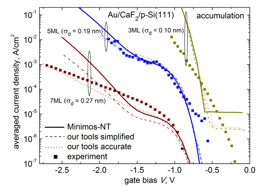
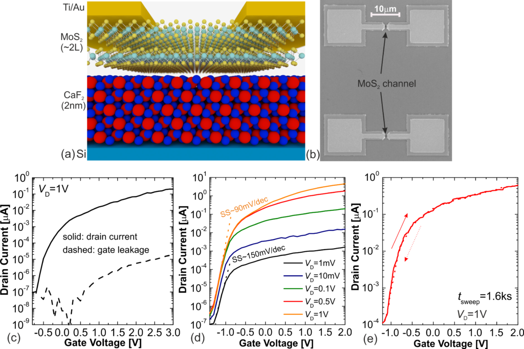
The research group is dealing with a study of properties and device applications of Metal – Insulator – Silicon (MIS) structures whose dielectric layer has a thickness of several nanometers, wherein a tunneling charge transport is possible. Until the beginning of the 2000s, the work of the group involved technology, measurement and theory parts with an approximately equal weight, however later the focus was shifted toward modeling. Special attention is paid to the points which are not so often touched in the traditional studies toward field-effect transistors. These are hot electron injection, co-existence of electron and hole tunnel components, parameter fluctuation problems, heavy-doped MIS structures, features of the crystalline insulators. Beyond the most popular insulator SiO2, also CaF2, Si3N4, Al2O3, HfO2, La2O3 and some other materials as well as dielectric stacks, are investigated.
Main achievements:
- the group developed high-level home-made programs for simulation of tunneling in various MIS systems;
- the group contributed to the creation of an MoS2/CaF2/Si field-effect transistor with a 2D disulfide channel. This work was published in the top journals and attracted attention of the mass media.
Cooperation:
A large fraction of works is being done in framework of partnership with the colleagues (Epitaxial dielectrics group at the Ioffe Institute, TU Vienna, TU Braunschweig etc.) interested in getting detailed theoretical information about the expected behavior of MIS tunnel systems with the specified material combinations.
Some illustrations:
Some publications:
- Determination of the hole effective mass in thin silicon dioxide films by means of an analysis of characteristics of a MOS tunnel emitter transistor // Vexler M.I., Tyaginov S.E., Shulekin A.F. // Journal of Physics: Condensed Matter, v. 17, № 50, pp. 8057-8068 (2005).
- A general simulation procedure for the electrical characteristics of metal-insulator-semiconductor tunnel structures // Vexler M.I., Tyaginov S.E., Illarionov Y.Y., Fedorov V.V., Isakov D.V., Sing Y.K., Shenp A.D. // Semiconductors, v. 47, № 5, pp. 686-694 (2013).
- Statistical analysis of tunnel currents in scaled MOS structures with a non-uniform oxide thickness distribution // Tyaginov S.E., Vexler M.I., Shulekin A.F., Grekhov I.V. // Solid-State Electronics, v. 49, № 7, pp. 1192-1197 (2005).
- Ultrathin Calcium Fluoride Insulators for Two-Dimensional Field-Effect Transistors // Illarionov Yu.Yu., Banshchikov A.G., Polyushkin D.K., Wachter S., Knobloch T., Thesberg M., Stoeger-Pollach M., Steiger-Thirsfeld A., Vexler M.I., Waltl M., Sokolov N.S., Mueller T., Grasser T. // Nature Electronics, v. 2, pp. 230-235 (2019).
- Insulators for 2D Nanoelectronics: the Gap to Bridge // Illarionov Yu.Yu., Knobloch T., Lanza M., Akinwande D., Vexler M.I., Mueller T., Lemme M., Fiori G., Schwierz F., Grasser T. // Nature Communications, v. 11, 3385 (2020).
Contacts:
| M.I. Vexler | vexler@mail.ioffe.ru | +7 (812) 292-71-23 |
| Yu.Yu. Illarionov | ill-88@mail.ru | +7 (812) 292-73-21 |
| S.E. Tyaginov | tyaginovs@gmail.com | +7 (812) 292-73-21 |