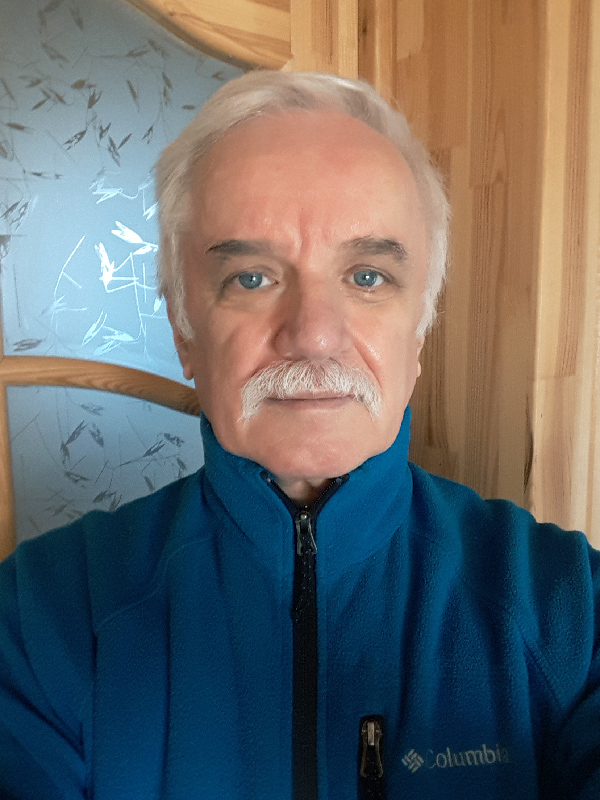
Dr.Sci. leading researcher. Deceased on January 19, 2023

Ivanov Pavel was one of the leading experts in Russia in physics and technology of SiC-based high-power and pulse devices. Developments and experimental studies of P.A. Ivanov and his group include world’s first junction field effect transistors (JFET, 1988-1989), MOS-transistors with accumulation n-channel (MOSFET), field-effect transistors with Schottky gate (MESFET), world’s first pulse power subnanosecond SiC devices such as high voltage drift step recovery diodes (DSRD), high voltage diodes with integrated Schottky-(p-n) structure (JBS), high voltage fast-recovery diodes (UFAD) operating in the regime of powerful controlled avalanche breakdown.
P.A. Ivanov has performed detailed experimental studies of electron processes in bipolar SiC devices including diodes, transistors and thyristors. He has developed analytical theory of surface capacitance for semiconductors with deep dopant impurities, analytical theory of power SiC accumulation-type MOSFET, analytical model of DSRD. P.A. Ivanov has performed numerical simulations of SiC devices transients with account taken for incomplete ionization of the dopant impurities and numerical simulations of electrostatic and thermal fields in SiC diodes. He has developed new methods of extracting the parameters of the surface states at the SiO2/SiC interface and performed experimental studies of electron drift in strong electric fields.
P.A. Ivanov has participated in various international research and technological projects (ISTC, CRDF) and had an extensive experience of international cooperation (Industrial Microelectronic Center (Stockholm, Sweden), Sandia National Laboratories (Albuquerque, NM), Air Force Research Laboratories (Albuquerque, NM), Сree Inc. (Durham, NC), Rensselaer Polytechnic Institute (Troy, NY), University of South Carolina (Columbia, SC)). P.A. Ivanov has participated (as a leader and executor) in the projects financed by the Ministry of Defense, Ministry of Industry, Ministry of Education and Science, RSBR, RAS, RSF. P.A. Ivanov has implemented and transferred to the industry (“KREMNIY-L”, Bryansk) the technology of SiC based JBS-diode manufacturing that has been developed under his supervising at the Ioffe Institute. P.A. Ivanov was an expert of RAS, expert of the Ministry of Education and Science, expert of the “Energy without boundaries” foundation, adviser of the Nanotechnology and Nanomaterials Center of the Republic of Mordovia and Bryansk State University.
He has over 2400 citations, H-index is 23 (according to Elibrary).

